Advancing Human History through
the Power of Diamond Semiconductors


BEYOND
DISASTER


OUR STORY
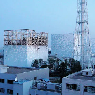
A national crisis sparked
a collective resolve
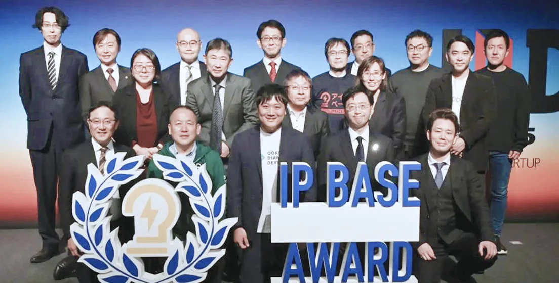
In the wake of Japan’s nuclear disaster, some of the nation’s brightest minds came together to confront a historic challenge: nuclear decommissioning. This is the story of how that moment led to the founding of Ookuma Diamond Device — a company born not merely to build semiconductors, but to create the next generation of them.
MISSION
Creating a next-generation semiconductor industry from Japan through the decommissioning of Fukushima Daiichi Nuclear Power Plant
Founded in the wake of the Great East Japan Earthquake, our company is driven by a mission to bring diamond semiconductors into practical use and contribute to society through their real-world deployment.

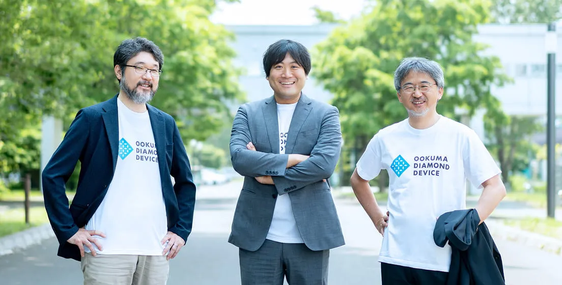
TECHNOLOGY
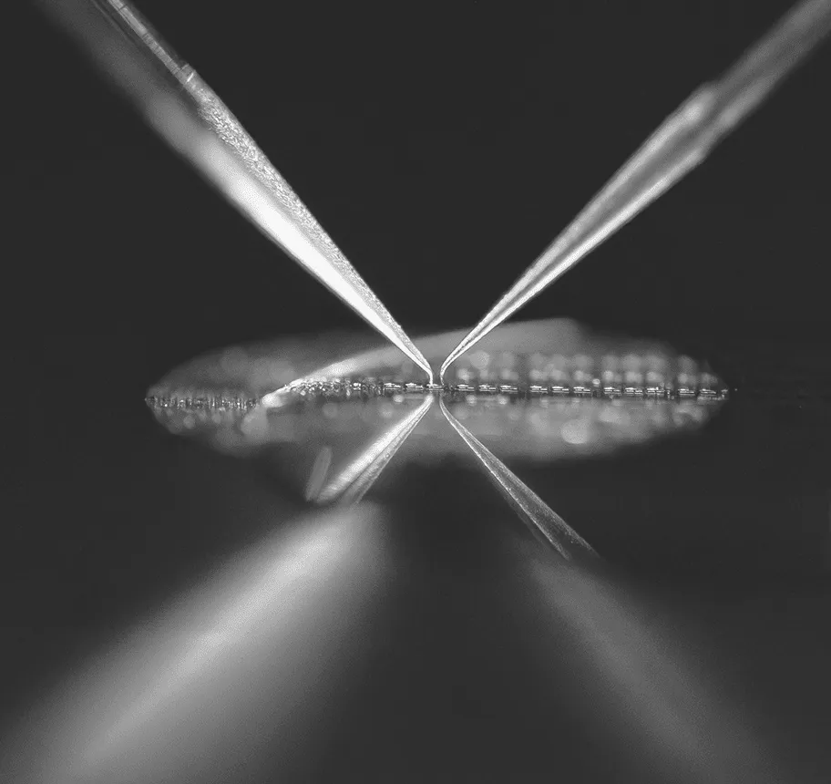
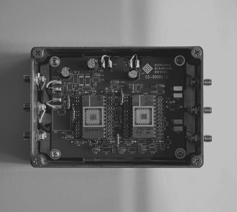
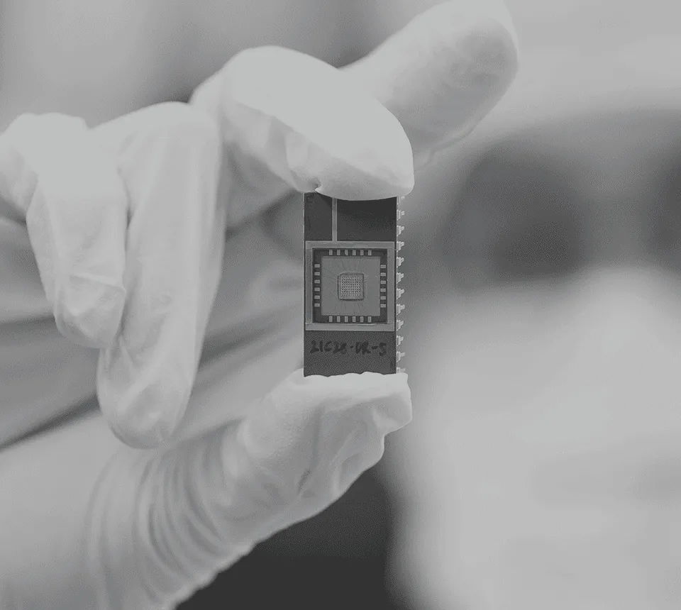
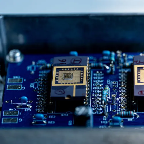
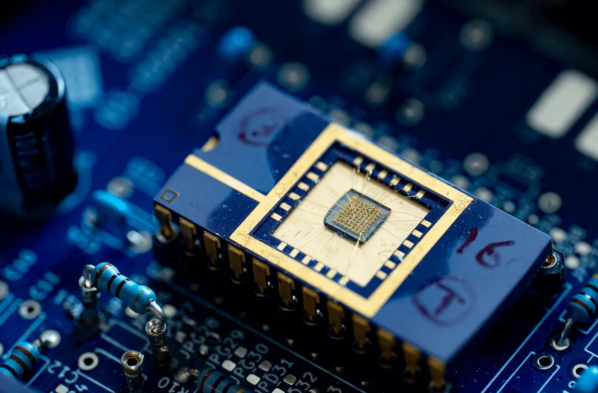
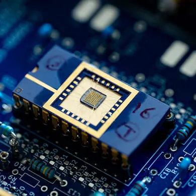
Celebrated for its extraordinary performance, diamond is often referred to as the ultimate semiconductor.
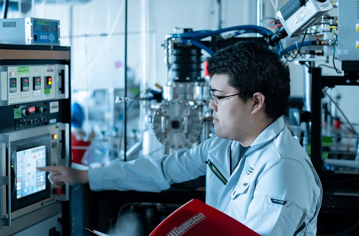
Ookuma Diamond Device was among the first to initiate full-scale pilot-line development to bring this technology into practical reality. Behind this effort lies over a decade of accumulated wisdom and achievement from Japan’s scientific community, forged through relentless pursuit of a singular goal: to overcome the global challenge of nuclear decommissioning.

Integration into Society


PROJECTS
We are working collaboratively with a wide range of government agencies on multiple projects. Research and development led by Ookuma Diamond Device to create Japan’s next-generation semiconductor industry is expected to play a vital role in shaping the future of society.
Key partner institutions
- Cabinet Office
- Ministry of Economy, Trade and Industry
- Ministry of Internal Affairs and Communications
- Reconstruction Agency
- Acquisition, Technology & Logistics Agency
- Fukushima Prefecture
- Japan Atomic Energy Agency
Private Companies / Others