Our Technological Edge
10-year decommissioning
project driven
by Japan’s leading minds
10-YEAR DECOMMISSIONING PROJECT
Our strength lies in over a decade of R&D experience dedicated to the unprecedented global challenge of nuclear decommissioning—an effort that has brought together Japan’s leading scientific minds. Through this journey, we have built vertically-integrated manufacturing expertise—from substrate design to the final assembly of amplifier modules.

Insights gained through decommissioning
and dialogue with the market
-
Consolidating dispersed expertise
Following the Fukushima Daiichi accident, a national project was launched to develop diamond semiconductors. Leading researchers across Japan—including our co-founders, Kaneko and Umezawa—joined forces in this collective effort.
-
Clear development targets
Successful decommissioning requires semiconductors that can operate in extreme conditions. This real-world demand has defined clear, tangible goals, driving the development of diamond semiconductor devices.
-
Practical design aiming
for mass productionOur goal is not merely academic achievement—we are committed to R&D that leads to real-world implementation. We focus daily on improving yield to ensure manufacturability and scalability of our products.
Verticaly
integrated
manufacturing
VERTICALY INTEGRATED
MANUFACTURING
Practical implementation requires not only improved performance but also high yield. To achieve both, it is essential to take a holistic view of the entire manufacturing process and optimize each step accordingly. However, because each production cycle takes time, completing even a single PDCA loop can take several months. Full validation and optimization of the entire flow often requires years. For this reason, achieving both performance and yield improvement is impossible without not only technological superiority but also a lead in time.

Through more than a decade of trial and error, even before our official founding, we have built the world's only vertically-integrated expertise in diamond semiconductor manufacturing. This has enabled us to achieve over 90% yield at the lab scale. Over the past decade, our pursuit of solutions for nuclear decommissioning has driven not only R&D but also ongoing dialogue with market stakeholders. This has led to the construction of the world’s first diamond semiconductor pilot line and is now accelerating the path to commercialization.
Building the world’s first pilot plant for diamond semiconductors
THE WORLD'S FIRST PILOT PLANT FOR DIAMOND SEMICONDUCTOR
we raised a total of ¥7.4 billion within three years of founding.
(As of June 2025, including contracted funding)
We have raised a total of approximately ¥7.4 billion (approx. USD 50 million as of September 2025), including investments from Japan’s leading venture capital firms such as Globis Capital Partners and Coral Capital, as well as government grants and public-sector funding. Backed by strong confidence from both domestic and international stakeholders, we have officially begun construction of the world’s first diamond semiconductor fabrication facility.
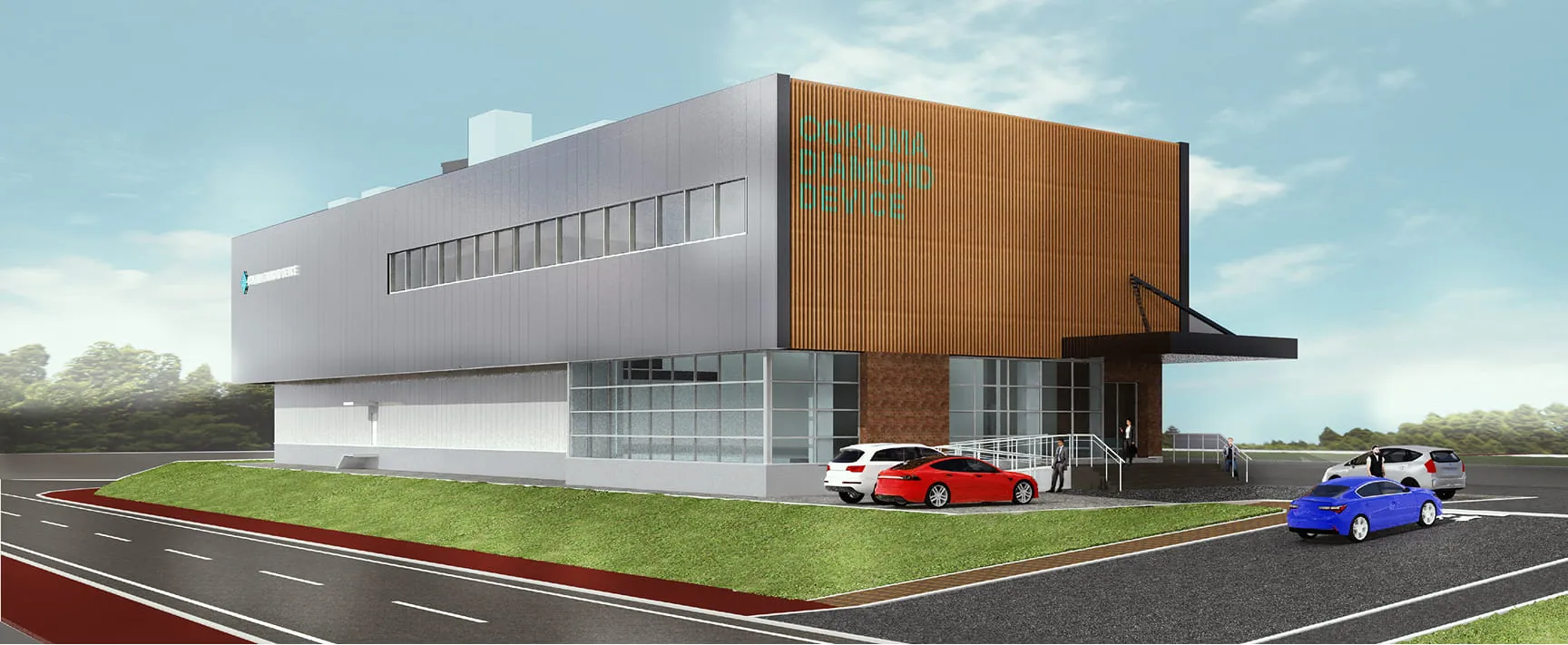
The facility is being built in Okuma Town, Futaba District, Fukushima Prefecture—the site of the Fukushima Daiichi Nuclear Power Plant. Construction began in fiscal year 2024 and is scheduled for completion in fiscal year 2026.
Through large-scale production of diamond semiconductors, we aim not only to support nuclear decommissioning but also to pioneer a next-generation semiconductor industry originating from Japan.