OUR STORY
INDEX
Why Diamond Semiconductors, and Why Now?
The "ultimate semiconductor”
that humanity has been waiting for.
Diamond semiconductors, often called the “ultimate semiconductor” for their exceptional performance, offer unique advantages in addressing critical challenges across nuclear energy, space development, and telecommunications. Once full-scale commercialization begins, they are expected to see widespread adoption in applications such as communication satellites, base stations, and electric vehicles.
1980s~
A Brief History of Diamond Semiconductor Research
Diamond semiconductor research has progressed step by step toward the future.
Researchers began investigating diamond semiconductors as early as the 1980s, recognizing their unique material properties. However, progress toward real-world deployment stalled due to both technical hurdles and the lack of a suitable market that could fully utilize these properties.
The origins of diamond semiconductor research can be traced back to 1982, when Japan’s former National Institute for Research in Inorganic Materials (now NIMS) succeeded in the world’s first diamond synthesis through Chemical Vapor Deposition (CVD). CVD is a technique that produces solid materials through chemical reactions in the gas phase, using hydrogen gas and methane gas containing carbon as source materials. While research accelerated globally in the years that followed, Japanese institutions such as NIMS and the National Institute of Advanced Industrial Science and Technology (AIST) played central roles in its development. Many researchers who believed in the future of diamond semiconductors made steady progress over the decades. Still, their efforts remained largely focused on elemental technologies, with diverse and often exploratory objectives. The path to real-world deployment was distant and uncertain. What changed everything was the Great East Japan Earthquake on March 11, 2011—a moment that redefined the urgency and direction of this technology’s application.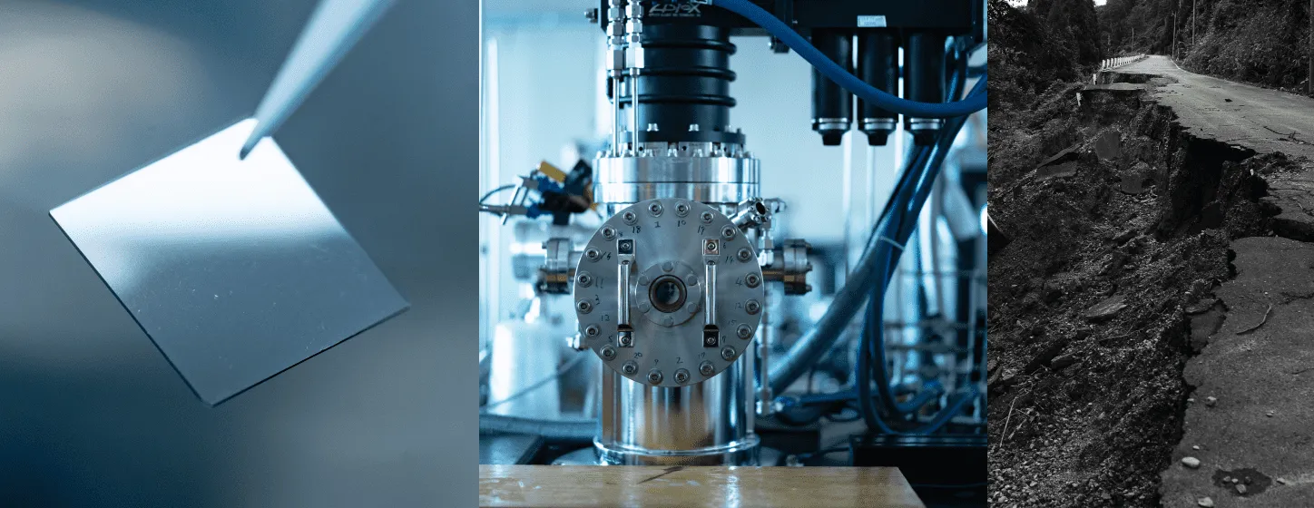
The origins of diamond semiconductor research can be traced back to 1982, when Japan’s former National Institute for Research in Inorganic Materials (now NIMS) succeeded in the world’s first diamond synthesis through Chemical Vapor Deposition (CVD). CVD is a technique that produces solid materials through chemical reactions in the gas phase, using hydrogen gas and methane gas containing carbon as source materials. While research accelerated globally in the years that followed, Japanese institutions such as NIMS and the National Institute of Advanced Industrial Science and Technology (AIST) played central roles in its development. Many researchers who believed in the future of diamond semiconductors made steady progress over the decades. Still, their efforts remained largely focused on elemental technologies, with diverse and often exploratory objectives. The path to real-world deployment was distant and uncertain. What changed everything was the Great East Japan Earthquake on March 11, 2011—a moment that redefined the urgency and direction of this technology’s application.
2011.3.11~
The Great East Japan Earthquake and the Fukushima Daiichi Nuclear Disaster
A unified mission accelerates development and brings scattered expertise together.
The accident at the Fukushima Daiichi Nuclear Power Plant marked a turning point, dramatically accelerating the path toward the practical application of diamond semiconductors. As Japan faced the unprecedented challenge of retrieving melted nuclear fuel debris as part of the decommissioning process, attention turned to the remarkable radiation tolerance of diamond semiconductors—materials capable of surviving in extreme environments. In 2012, just a year after the accident, a national project was launched to develop diamond semiconductors.
The project was led by the Japan Atomic Energy Agency (JAEA), with participation from institutions such as AIST, Hokkaido University, and the High Energy Accelerator Research Organization (KEK). It also served as the catalyst that brought our co-founders—Hoshikawa, Kaneko, and Umezawa—together as a team. As the need for semiconductors capable of withstanding extreme environments became a national imperative, diamond semiconductors were officially recognized as critical to public interest. This led to the consolidation of previously scattered knowledge and expertise from multiple research institutions into a unified development effort.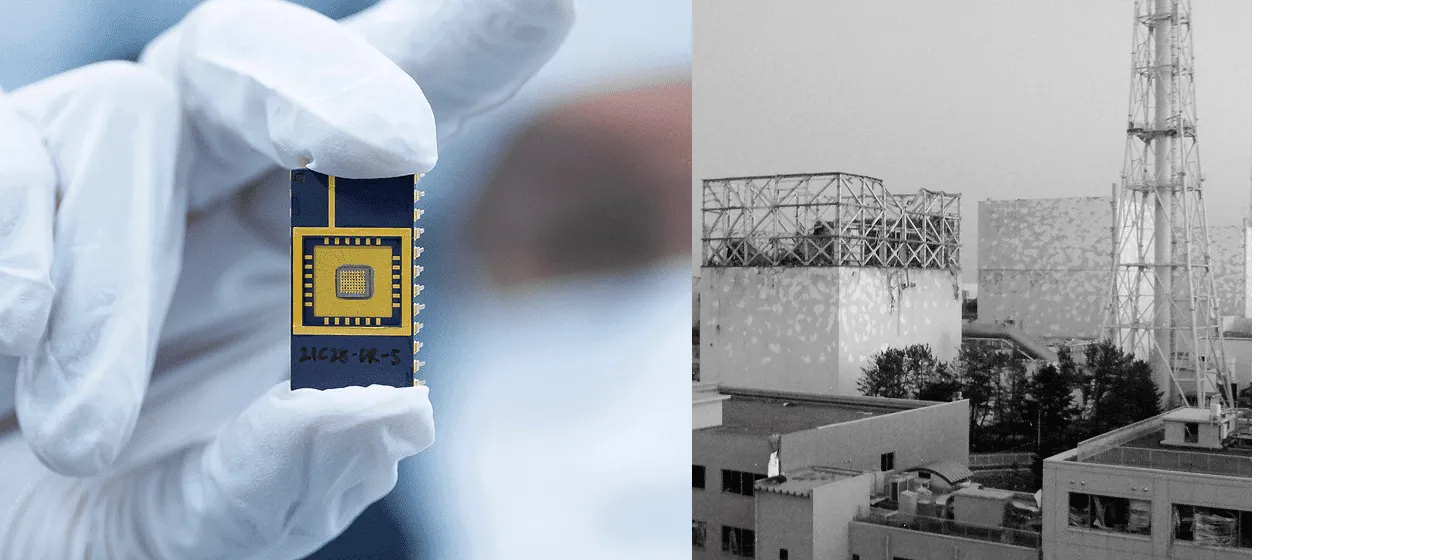
The project was led by the Japan Atomic Energy Agency (JAEA), with participation from institutions such as AIST, Hokkaido University, and the High Energy Accelerator Research Organization (KEK). It also served as the catalyst that brought our co-founders—Hoshikawa, Kaneko, and Umezawa—together as a team. As the need for semiconductors capable of withstanding extreme environments became a national imperative, diamond semiconductors were officially recognized as critical to public interest. This led to the consolidation of previously scattered knowledge and expertise from multiple research institutions into a unified development effort.
2022~
Founding of Ookuma Diamond Device
To transform the collective wisdom of Japan into tangible outcomes, Ookuma Diamond Device was founded.
In 2021, a major milestone was reached when Japan’s concentrated research efforts culminated in the world’s first successful prototype of a diamond semiconductor amplifier—an achievement aimed at addressing the national challenge of nuclear decommissioning. A decade of collaborative research had borne significant fruit. However, there remained no organization capable of scaling the manufacturing and mass production of diamond semiconductors, leaving a critical gap between technical success and practical deployment. It was to break through this impasse that Hoshikawa, now CEO of Ookuma Diamond Device, stepped forward. A serial entrepreneur who launched his first startup while still a student at Hokkaido University, Hoshikawa had already built a track record across multiple fields. In 2016, he encountered Professor Kaneko’s lab and was deeply moved by both the mission of the decommissioning project and the future potential of diamond semiconductors. Driven by a sense of purpose, he volunteered to join the effort and took on a central role in productization and operational leadership from the project's inception.
Joining Hoshikawa as co-founders were two of Japan’s leading researchers in the field. One was Professor Kaneko, an associate professor at Hokkaido University, who also served at the time as group leader at the JAEA’s International Collaborative Research Center for Decommissioning, where he played a key role in Japan’s post-accident response. The other was Dr. Umezawa, a senior principal researcher at AIST and a globally recognized authority in diamond semiconductors. In 2022, these three individuals came together to establish Ookuma Diamond Device—an organization dedicated to the commercialization and mass production of diamond semiconductor devices.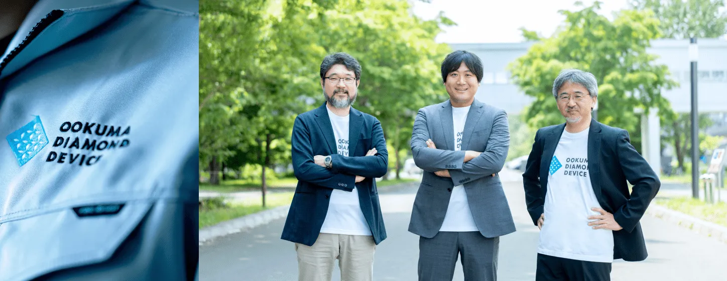
Joining Hoshikawa as co-founders were two of Japan’s leading researchers in the field. One was Professor Kaneko, an associate professor at Hokkaido University, who also served at the time as group leader at the JAEA’s International Collaborative Research Center for Decommissioning, where he played a key role in Japan’s post-accident response. The other was Dr. Umezawa, a senior principal researcher at AIST and a globally recognized authority in diamond semiconductors. In 2022, these three individuals came together to establish Ookuma Diamond Device—an organization dedicated to the commercialization and mass production of diamond semiconductor devices.
WHAT’S NEXT
Where We Stand on the Path to Real-World Deployment
Building on a foundation of overwhelming technical expertise developed even before its founding, Ookuma Diamond Device is constructing the world’s first diamond semiconductor manufacturing plant in Okuma, Fukushima.
Through over a decade of continuous trial and error even before its founding, Ookuma Diamond Device succeeded in developing the world’s only fully vertically-integrated manufacturing expertise for diamond semiconductors. This capability has enabled us to achieve a yield rate exceeding 90% at the laboratory scale. Over the ten years spent addressing the critical national challenge of nuclear decommissioning, our work extended beyond research and development. It fostered meaningful dialogue with emerging markets that seek diamond semiconductors, accelerating the path toward practical implementation.
After more than a decade of confronting the uniquely Japanese challenge of nuclear decommissioning, Ookuma Diamond Device has established a level of technical superiority that is expected to remain unmatched for years to come. It now stands as the world’s only entity within reach of building a fully operational diamond semiconductor plant. To fulfill its founding mission, the company is currently constructing the world’s first such facility in Okuma, Fukushima—the very town where the Fukushima Daiichi Nuclear Power Plant is located. The plant is scheduled for completion in 2026. This undertaking not only reinforces the company’s technological edge, but also lays a firm foundation for the emergence of a next-generation semiconductor industry originating from Japan.

After more than a decade of confronting the uniquely Japanese challenge of nuclear decommissioning, Ookuma Diamond Device has established a level of technical superiority that is expected to remain unmatched for years to come. It now stands as the world’s only entity within reach of building a fully operational diamond semiconductor plant. To fulfill its founding mission, the company is currently constructing the world’s first such facility in Okuma, Fukushima—the very town where the Fukushima Daiichi Nuclear Power Plant is located. The plant is scheduled for completion in 2026. This undertaking not only reinforces the company’s technological edge, but also lays a firm foundation for the emergence of a next-generation semiconductor industry originating from Japan.
*Yield percentage based on the ratio of manufactured transistors that exhibited functional operation.
OUR VISION
The Future Opened Up by Diamond Semiconductors
Creating a next-generation semiconductor industry from Japan through the decommissioning of Fukushima Daiichi Nuclear Power Plant
The potential of diamond semiconductors extends far beyond their contributions to nuclear decommissioning. Their ability to withstand extreme conditions—including high and low temperatures, as well as radiation—combined with exceptional high-frequency and high-power efficiency, makes them valuable in addressing pressing challenges in nuclear energy, space exploration, and next-generation communications. Moreover, their energy-saving characteristics surpass what is achievable with conventional semiconductor technologies, positioning them as a key enabler of a decarbonized society. From advancing communication satellites to realizing future network technologies, diamond semiconductors are expected to serve as a critical foundation for the next-generation information infrastructure.
For us, true recovery is not merely about bringing a negative back to zero. It lies in creating new industries from adversity and turning that experience into a lasting positive. By harnessing diamond semiconductors to move beyond the legacy of the nuclear accident, and by building upon the technologies cultivated in that process, we believe humanity can take its next step forward. This is the future we strive to realize. Through the decommissioning of the Fukushima Daiichi Nuclear Power Plant, we are committed to building a next-generation semiconductor industry originating from Japan.
For us, true recovery is not merely about bringing a negative back to zero. It lies in creating new industries from adversity and turning that experience into a lasting positive. By harnessing diamond semiconductors to move beyond the legacy of the nuclear accident, and by building upon the technologies cultivated in that process, we believe humanity can take its next step forward. This is the future we strive to realize. Through the decommissioning of the Fukushima Daiichi Nuclear Power Plant, we are committed to building a next-generation semiconductor industry originating from Japan.